
The intricacy of electronic devices’ functionality in compact designs has long been a mystery. The emergence of multilayer PCBs has presented a viable solution to a long-standing challenge. Drawing a parallel to a multi-level building, where each floor is allocated a particular role, such as living, dining, and sleeping, the multilayer PCBs are comprised of several layers that fulfill distinct functions.
This innovative technology has transformed the field of electronics by enabling superior performance and compact designs. These intricate circuit boards provide more space for components and enable better signal integrity and reduced electromagnetic interference.
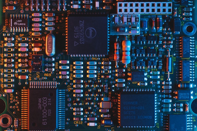
From smartphones to medical equipment to automotive systems, multilayer PCBs play a crucial role in powering our everyday devices. You can check NextPCB reliable multilayer PCB manufacturer for your needs.
This post and content offer an exhaustive examination of the sophisticated architecture, design tenets, manufacturing methods, and versatile applications pertaining to multilayer printed circuit boards. Whether you are an aspiring technologist or harbor a deep fascination for the mechanics of your electronic gadgets, we extend a cordial invitation to you to embark on a gripping odyssey into the realm of multilayer PCBs.
Understanding the Structure of Multilayer PCBs
Multilayer PCB’s benefits are endless. They provide higher circuit density, allowing for more components to be placed on a smaller board. This leads to reduced size and weight of electronic devices, making them more compact and portable. Incorporating multiple power and ground planes, multilayer printed circuit boards (PCBs) provide improved signal integrity and electrical performance, rendering them a superior option in comparison to their single-layer counterparts.
The increased complexity requires careful consideration of factors like layer stack-up design, impedance control, and signal integrity issues. Ensuring proper power distribution across layers is crucial to prevent noise interference and cross-talk between signals. Furthermore, managing heat dissipation becomes vital as it can affect the overall reliability and performance of the PCB.
While multilayer PCBs offer significant advantages in terms of circuit density and performance, designers must overcome various challenges to optimize their functionality.
Design Considerations for Multilayer PCBs
Moreover, the intricate process of developing a multilayer printed circuit board necessitates a comprehensive consideration of a plethora of influential factors.One important consideration is thermal management. With multiple layers stacked on top of each other, heat dissipation becomes a challenge. To address this, designers must carefully plan the placement of components and consider adding thermal vias or copper planes to efficiently transfer heat away from critical areas.
Another key aspect is signal integrity. As signals travel through different layers and traces, they can encounter impedance mismatches or noise interference. Designers need to pay attention to trace widths, and spacing between them, and use techniques like controlled impedance routing to ensure reliable signal transmission.
By taking these design considerations into account, engineers can create multilayer PCBs that effectively manage heat dissipation while maintaining optimal signal integrity for high-performance applications.
The Manufacturing Process of Multilayer PCBs
To successfully bring a multilayer PCB to life, engineers embark on a meticulous process that involves intricate layer alignment, precise etching techniques, and advanced assembly methods.
The manufacturing process of multilayer PCBs begins with the lamination process, where multiple layers of copper foil and dielectric material are pressed together under high temperature and pressure. This ensures proper bonding and electrical insulation between the layers.
Quality control plays a crucial role in multilayer PCB production. It involves thorough inspection at various stages to identify any defects or inconsistencies in the manufacturing process. This includes checking for proper layer alignment, conducting electrical tests to ensure signal integrity, and inspecting for any visible defects such as cracks or delamination.
Implementing stringent quality control measures is essential to ensure the reliable performance and functionality of the final product.
Applications of Multilayer PCBs in Electronic Devices
You’ll find that electronic devices in various industries heavily rely on the complex and versatile capabilities of these multi-layered circuit boards.
Multilayer PCBs offer numerous benefits and advantages, making them popular in many applications. The compact size of multilayer printed circuit boards (PCBs) presents a major advantage for modern electronic devices, enabling more components to be accommodated within a confined space.
This feature not only optimizes valuable real estate but also minimizes the overall weight of the device. Multilayer Printed Circuit Boards (PCBs) provide enhanced signal integrity by reducing the interference caused by noise and crosstalk across multiple layers.
Conclusion
Congratulations! You’ve now explored the fascinating world of multilayer PCBs. These intricate circuit boards are like the beating heart of modern electronic devices, seamlessly connecting components and bringing them to life.
Just like an artist paints layer upon layer to create a masterpiece, multilayer PCBs weave their magic by stacking multiple layers of circuits together.
So next time you hold a cutting-edge gadget in your hands, remember the hidden marvel that lies within – the multilayer PCB.