
In today’s fast-paced technological landscape, high-speed applications are becoming increasingly prevalent. Whether it’s in the realm of telecommunications, data processing, or advanced electronics, achieving reliable and efficient signal transmission is paramount. One crucial element in ensuring signal integrity, power distribution, and noise reduction is the design of the printed circuit board (PCB). In this article, we will explore the advantages and challenges of using 4 layer PCB for high-speed applications and provide insights into best practices for their design.
Understanding 4 Layer PCBs
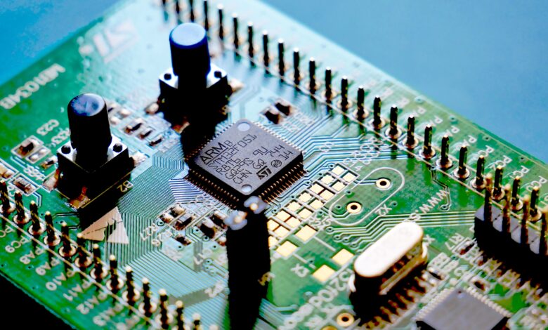
A 4 layer PCB as the name suggests consists of four layers of conductive material separated by the dielectric layers. These PCBs differ from they single and double-layer counterparts by offering additional routing and grounding options. The four layers typically consist of:
- Top Layer: This is where most of the components and signal traces are placed.
- Inner Signal Layers (L2 and L3): These layers contain signal traces and are separated by a dielectric material. They enable complex routing for high-speed signals.
- Bottom Layer: Similar to the top layer, it accommodates components and signal traces.
- Ground Plane (L4): The ground plane provides a solid reference for signal return paths and helps minimize electromagnetic interference (EMI).
Advantages of 4-Layer PCBs
- Signal Integrity Enhancement
The primary advantage of using a 4 layer PCB for high speed applications is the significant improvement in signal integrity. By having dedicated signal layers and the ground plane you can minimize crosstalk impedance mismatches and signal distortions. This translates into cleaner and more of reliable signal transmission critical for applications such as the high frequency data transfer and radio frequency (RF) communications.
- Power Distribution Efficiency
High-speed applications often demand precise and stable power distribution. With a 4 layer PCB, you can create dedicated power planes, ensuring that critical components receive consistent power without interference from signal traces. This improves the overall efficiency and performance of your circuit, particularly when dealing with power-hungry components like microprocessors and high-speed memory modules.
- Noise Reduction
Noise is the enemy of high-speed signal transmission. 4 Layer PCBs allow you to effectively manage noise by isolating signal layers from each other and providing a solid ground reference. This helps reduce electromagnetic interference and ensures that your circuit operates with minimal noise, crucial for sensitive analog circuits and high-speed digital interfaces.
Design Considerations and Best Practices
Creating a 4 layer PCB for high-speed applications requires careful planning and attention to detail. Here are some key design considerations and best practices:
- Stack-Up Design
The choice of stack-up is critical. Ensure that signal layers are placed between ground planes to provide a low-impedance path for return currents. Typical stack-ups include signal-ground-signal-power or signal-power-ground-signal. The specific stack-up depends on your application’s requirements and the frequencies involved.
- Impedance Matching
High-speed signals are sensitive to impedance discontinuities. Use controlled impedance traces and ensure that your PCB manufacturer can meet your specified impedance requirements. Tools like signal integrity simulators can help validate your design, ensuring that signals propagate with minimal distortion.
- Proper Routing
Routing high-speed signals should be done with care. Maintain consistent trace widths, minimize sharp corners, and follow best practices for differential pairs. Utilize ground vias strategically to connect signal layers to the ground plane. Additionally, consider using differential pair routing guidelines to minimize skew and ensure signal integrity for differential signals.
- Via Placement
Correct via placement is crucial for signal integrity. Place vias close to the signal traces they connect and avoid stubs that can introduce impedance mismatches. Blind and buried vias can also be employed for complex routing. Proper via placement is essential for maintaining signal integrity and minimizing signal reflections.
- Ground Plane Management
Ensure the ground plane is continuous and unbroken. Avoid splitting it with traces or components, as this can lead to ground loops and EMI issues. Use stitching vias to connect different sections of the ground plane together, creating a solid reference plane that minimizes ground bounce and EMI.
- EMI Mitigation
Implement EMI shielding techniques like adding ground planes above and below signal layers or using shielding cans over sensitive components. This helps reduce the emission of electromagnetic interference, ensuring compliance with electromagnetic compatibility (EMC) standards.
- Thermal Management
High-speed applications can generate heat, especially when dealing with high-performance processors and integrated circuits. Plan for adequate thermal management, including the placement of heat sinks, thermal vias, and thermal pads, to prevent overheating and ensure long-term component reliability.
- Signal Integrity Analysis
Before sending your design for fabrication, perform a thorough signal integrity analysis to identify and address potential issues. Tools like simulations and signal integrity analyzers can help you validate your design’s performance, ensuring that it meets your high-speed application’s requirements.
Conclusion
In high-speed applications, the use of a 4-layer PCB can significantly enhance signal integrity, power distribution efficiency, and noise reduction. These advantages make 4-layer PCBs a preferred choice for cutting-edge electronics. However, designing a 4-layer PCB requires careful consideration of stack-up, impedance matching, routing, via placement, ground plane management, EMI mitigation, thermal management, and signal integrity analysis.
The success of your high-speed circuit ultimately depends on the quality of your PCB design, so invest the time and effort required to get it right. By following best practices and paying attention to these critical aspects, you can create a 4 layer PCB that meets the demands of high-speed applications, ensuring reliable and efficient signal transmission.